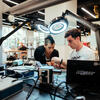
The College is continuously investing in resources in order to provide the best education and advancements through research. Our more than 20 labs, institutes and centers and more than a dozen teaching labs are home to state-of-the-art equipment and tools.

Temple Engineering recently debuted the Innovation, Design, Engineering and Applied Science (IDEAS) Hub, an 8,000 square-foot renovation that is part of a collaborative ecosystem in the College. The IDEAS Hub will empower students to use engineering for good. From 3D printing, motion capture and drone stations to robotics, soldering an circuitry, our students and faculty have the tools to do more than learn engineering, they can now make their ideas for changing the world a reality.
Other dedicated teaching, student and user accessible labs have equipment ranging from flourescent microscopes, materials testing equipment, asphalt ovens, concrete mixing, digital simulators and microwave detectors to machining equipment for building or studying impact. The college also has top of the line facilities that can be accessed by students and faculty in and out of the College. The nanoinstrumentation center and system design chip laboratory are just a few of the dedicated spaces available for engineers to do their work.
Research facilities
Our 800-sq ft facility, located in Department of Civil and Environmental Engineering, is equipped to conduct experimentation in the field of microbiology, phytotechnology, and molecular biology. The laboratory also owns advanced analytical equipment and is equipped for working under sterile conditions. An additional 300-sqft growth room contains various incubators and lighted shelves for growing bacteria, algae, and plants.
MAJOR EQUIPMENT:
- Five-color real-time PCR system (Applied Biosystems)
- Electrophoresis units and UV transilluminator 32-L vertical-loading autoclave
- Four-foot Class II Biosafety laminar-flow cabinet 2 six-foot chemical hoods
- Anaerobic glove box with automatic airlock and vacuum pump (Coy Lab)
- Lighted shelves equipped with cold white fluorescent tubes for plant growth
- Gas chromatograph-mass spectrometer (Agilent 7890A GC - 5975C MSD/DS)
- High performance liquid chromatograph (Agilent 1260 Infinity LC - Diode ArrayDetector VL)
- High resolution TOC analyzer (Shimadzu) 96-well microplate spectrofluorimeter (LJL Biosystem)
- UV-visible spectrophotometer with PDA (Agilent 8453)
- Nanopure water, liquid nitrogen, and ice
One of the most comprehensive Scanning Electron Microscopes, the FEI Quanta 450FEG SEM, equipped with the latest Energy Dispersive Spectrometer (Oxford Aztec Energy Advanced EDS System) is housed in the College of Engineering. These Nanotechnology tools address the need to investigate a wide variety of materials and characterize structure and composition. The lab aims to to enhance the education, collaboration, research, and outreach related to all aspects of electron probe instrumentation, techniques and applications. The facility is multi-user and cross-departmental — open to any qualified scientist to use, with our qualified microscopist and material scientist Prof. Dmitriy Dikin and director Prof. Parsaoran Hutapea offering training and technical support.
KEY FEATURES:
- High resolution FEG-SEM with ESEM technology
- SE and BSE imaging in every mode of operation allowing for characterization of conductive and non-conductive samples
- Low vacuum and ESEM capability enables charge-free imaging and analysis of non-conductive and/or hydrated specimens allowing for minimized sample preparation
- Capable of EDS analysis on conductive and non-conductive samples in high and low vacuum
- Imaging with beam deceleration mode to get surface and compositional information from conductive samples
- Easy to use, intuitive software makes highly effective operation possible for novice users
- Possible additions: Perform dynamic in situ analysis of samples in their natural state above or below ambient temperatures from - 165 °C to 1000 °C with specialized in situ stages. High resolution bright and dark field imaging of thin slices of materials by scanning transmission electron detector (STEM). In situ mechanical and electrical measurements.
Visit the NIC page for more information and to make a reservation.
The SCDL is forging a new paradigm for the rapid design of complex digital systems, digital signal and image processing, digital communications and advanced processor systems in programmable gate arrays (PGA) reconfigurable system-on-chip (SOC) architectures utilizing behavioral analysis and synthesis and industry-standard digital design and embedded system computer aided (CAD) software tools.
Facilities for behavioral and hardware synthesis include the complete integrated synthesis environment (ISE) design suite from Xilinx executing on Windows XP/Vista and Linux PC engineering workstations. The SCDL is located in the College of Engineering Building on the Main Campus of Temple University, Philadelphia.
The SCDL is an Educational facility with a mandate to meld the traditional threads of digital logic design to the SOC paradigm of the PGA architecture in both undergraduate and graduate engineering education. Faculty and student resources are provided for this mission and for curriculum development.
Contact Prof. Dennis Silage or visit the System Chip Design Lab for more information.

